
Knowledge Center
Diamond in Semiconductor
The high-performance material in modern electronics, produced in our own machines.
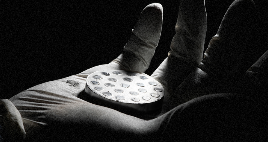
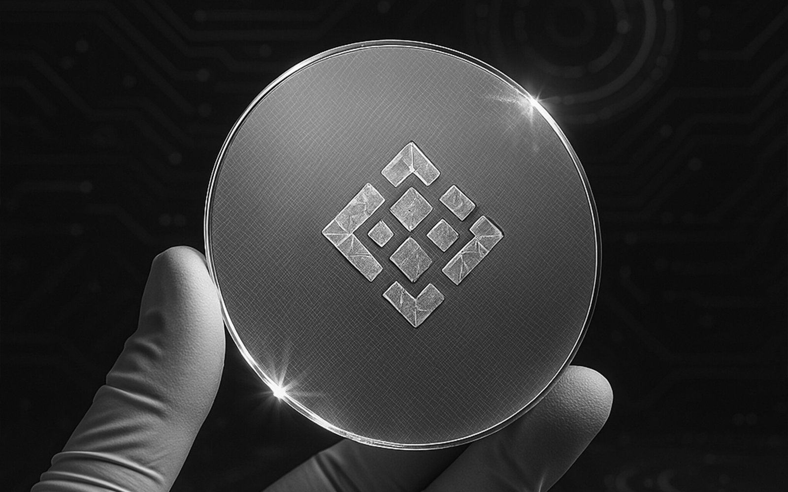
Lab-grown diamond substrates are thin diamond wafers used as base materials for growing single-crystal diamonds through the MPCVD and HPHT method. Their high thermal conductivity, exceptional hardness, wide bandgap, and broad optical transparency make them ideal for use in semiconductors, quantum computing, optics, lasers, and the gemstone industry.
“The high-performance material in modern electronics — produced in our own MPCVD machine.”
Applications
Applications Across High-Technology Industries

Diamond Semiconductor Substrates
High-quality CVD diamond substrates for advanced electronic and industrial applications, with superior reliability and thermal management.
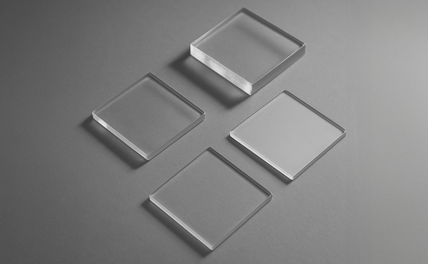
Diamond Heat Sinks
Thermal management for high-power devices — diamond significantly outperforms copper and aluminium in heat dissipation.
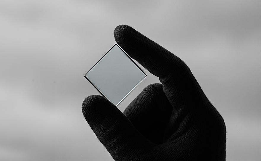
Diamond Heat Spreaders
Engineered for high thermal distribution — optimal for high-reliability applications where temperature management is critical.
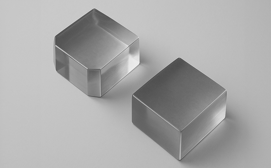
Optics
Custom diamond optics leveraging superior hardness, thermal conductivity, and clarity for demanding laser applications.
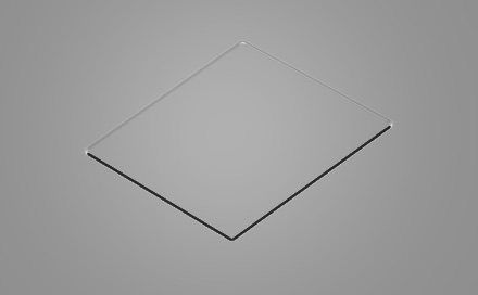
Mechanical Tooling
Diamond-based tooling offering higher durability and precision for industrial use where conventional materials wear prematurely.

Quantum Technologies
Unique quantum properties, including nitrogen-vacancy centres, make diamond a leading material for quantum computing and sensing.
Speak to Our Materials Science Team
For technical specifications, samples, and custom application support, our engineering team is available.